AI Stack Atlas / PM Edition
/

From silica to tokens

See the whole AI machine.

AI is not one supply chain. It is a set of nested production systems: materials become tools, tools make wafers, dies meet memory inside packages, packages mount onto boards, boards fill racks, and racks wait for power. Follow the constraint, then ask who owns the qualified capacity.

New deep dive: CPO Sector Atlas

A full cutaway of the ASIC, EIC, PIC, external laser, package substrate, PCB and fiber path—plus OCI/Open CPX/XPO, bottlenecks, company exposures and the updated production timeline.

Open CPO atlas →
01 / FLOWDemand starts downstreamModel use drives compute; compute architecture rewrites the bill of materials.
02 / CHOKEScarcity often sits upstreamA low-cost material can gate a high-value system if it is hard to qualify.
03 / CLOCKEvery layer runs on a different clockDesign wins, qualification, equipment orders, capacity, shipments, and revenue do not arrive together.
04 / P&LTechnical bottleneck is not enoughCheck segment mix, customer concentration, pricing power, and how much the theme can move earnings.

01 / End-to-end map

Where every term sits.

Select a node to see its job, common bottlenecks, the KPI trail, and representative companies. Arrows mean physical or economic dependency, not that every company buys directly from the next.

enabling inputs silicon and package systems and network deployment and demand

02 / Market heatmap crosswalk

Same chain, different lens.

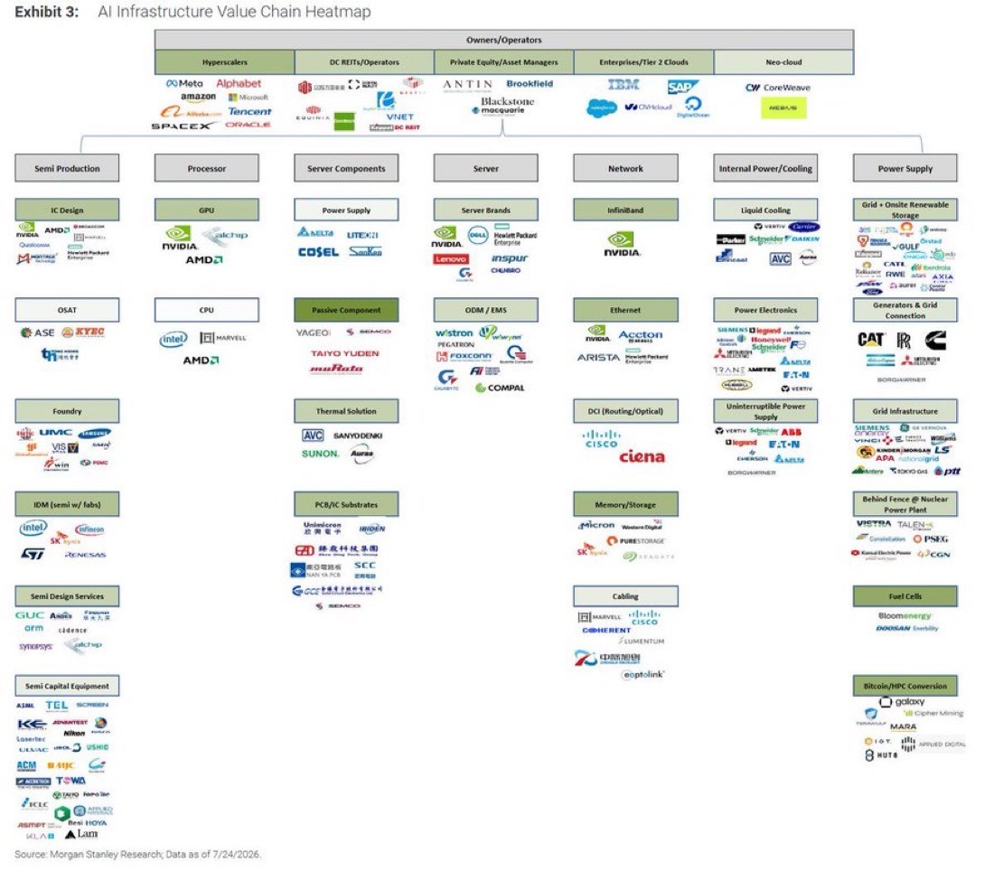
The Morgan Stanley exhibit organizes investable beneficiaries by owner and product bucket. The atlas organizes physical and economic dependency. This overlay reconciles every named box without pretending capital owners, manufacturing processes, and components are the same kind of node.

Morgan Stanley AI Infrastructure Value Chain Heatmap showing owners and operators above semiconductor production, processors, server components, servers, networking, internal power and cooling, and site power supply.
SUPPLIED REFERENCE · “AI INFRASTRUCTURE VALUE CHAIN HEATMAP” · SOURCE LABEL: MORGAN STANLEY RESEARCH · DATA AS OF 2026-07-24 · CLICK TO ENLARGE
already explicit previously compressed new edge case

Owners / operators

Who funds, owns or consumes the capacity

  • HyperscalersL12 · ALREADY EXPLICIT
  • DC REITs / operatorsL11–L12 · FACILITY OWNER / OPERATOR
  • Private equity / asset managersCAPITAL OVERLAY · PROJECT FINANCING
  • Enterprises / Tier 2 cloudsL12 · DEMAND AND UTILIZATION
  • NeocloudsL12 · ALREADY EXPLICIT

Semi production

Who designs and manufactures silicon

  • IC designL03 · FABLESS + IP
  • OSATL06 · ASSEMBLY + TEST SERVICES
  • FoundryL04 · CUSTOMER WAFER FABRICATION
  • IDML03–L06 · DESIGN + OWNED MANUFACTURING
  • Semiconductor design servicesL03 · CUSTOM IMPLEMENTATION + NRE
  • Semiconductor capital equipmentL02 · FAB TOOLS + PROCESS CONTROL

Processors

Compute engines inside the system

  • GPU / acceleratorL03–L06 · DESIGN THROUGH PACKAGE
  • CPUL03–L09 · HOST COMPUTE + SERVER

Server components

The board-level bill of materials

  • Server power supplyL08–L09 · AC/DC + POWER SHELF
  • Passive componentsL08 · MLCC + RESISTOR + INDUCTOR
  • Thermal solutionsL09–L11 · FANS + HEAT TRANSFER
  • PCB / IC substratesL07–L08 · DISTINCT PHYSICAL LAYERS

Servers

Who turns components into systems

  • Server brands / OEMsL09 · BRANDED SYSTEM + SUPPORT
  • ODM / EMSL09 · DESIGN, ASSEMBLY + SCALE

Network

How data and storage connect

  • InfiniBandL10 · SCALE-UP / SCALE-OUT FABRIC
  • EthernetL10 · SWITCHING + NETWORK OS
  • DCI routing / opticalL10 · SCALE-ACROSS BETWEEN SITES
  • Memory / storageL05 + L09 · ALREADY EXPLICIT
  • CablingL10 · COPPER, FIBER + CONNECTORS

Internal power / cooling

Inside the facility and rack

  • Liquid coolingL11 · COLD PLATE TO HEAT REJECTION
  • Power electronicsL08–L11 · CONVERT, REGULATE + PROTECT
  • Uninterruptible power supplyL11 · CONDITIONING + RIDE-THROUGH

Site power supply

How megawatts reach the data hall

  • Grid + onsite renewables + storageL11 · ENERGY SUPPLY PORTFOLIO
  • Generators + grid connectionL11 · BACKUP + INTERCONNECT
  • Grid infrastructureL11 · SUBSTATION, TRANSFORMER, SWITCHGEAR
  • Behind-the-meter / nuclear powerL11 · DEDICATED OR CONTRACTED GENERATION
  • Fuel cells + hot boxL11 · SOFC ONSITE GENERATION
  • Policy-qualified grid equipmentL11 · TRANSFORMER, SWITCHGEAR, UPS + CONTROLS
  • Bitcoin / HPC conversionL11–L12 · POWERED-SITE REPURPOSING

Coverage here means the component or ownership category is explicitly placed. It does not mean every logo in the exhibit is included, investable, correctly valued, or a pure-play beneficiary.

03 / The confusing middle

Glass cloth to PCB, in five moves.

This is where “substrate,” “laminate,” “board,” and “package” get mixed together. The same upstream chemistry and process logic can feed different products with very different tolerances.

Raw input

Glass yarn

Fine electronic-grade glass filaments spun from specialty glass compositions.

Woven input

Glass cloth

A woven reinforcement. Low-CTE and low-loss grades help control warpage and signal integrity.

Laminate

CCL

Copper-clad laminate: glass cloth impregnated with resin and bonded to copper foil.

Fabrication

PCB

CCL is patterned, drilled, plated, stacked, and laminated into a printed circuit board.

System

Server board

The PCB carries GPUs, CPUs, networking, power stages, connectors, and thousands of passives.

“Clean electric cloth” is probably electronic glass cloth.

The market usually means electronic-grade glass fiber cloth, sometimes specifically low-CTE glass cloth such as T-glass. It is not a cleanroom wipe and it is not copper foil. It reinforces CCL, which is then processed into PCB. When AI boards become larger, faster, hotter, and more multilayered, flatter and lower-loss cloth can become a qualification bottleneck.

PTFE · Q-glass · M9 / M10

The note mixes ingredients, a finished material and a performance label.

Think of high-speed CCL as a sandwich recipe. The resin controls much of the electrical loss, the cloth keeps the sheet stable, and the copper carries the signal. The exact qualified recipe—not one ingredient alone—determines who wins the board socket.

DO NOT MIX THE LAYERS
PTFE is a resin. Q-glass is a reinforcement cloth. CCL is the finished laminate. M9/M10 are performance-generation shorthand. ABF belongs in the IC package substrate below the chip package, not in the server-board CCL stack.

Reinforcement

E-glass, T-glass or Q-glass

Woven fibers hold the laminate together and control expansion. Q-glass means quartz cloth: lower dielectric loss and expansion than ordinary electronic glass, but harder processing and qualification can raise cost.

Q-GLASS IS A TYPE OF ELECTRONIC CLOTH

Resin system

Epoxy, PPE/PPO, hydrocarbon or PTFE

Resin fills the cloth and electrically insulates copper layers. PTFE is a real ultra-low-loss option, but it can be harder to bond, drill and laminate than familiar thermoset systems.

PTFE IS CHEMISTRY, NOT A COMPANY OR BOARD

Conductor

Low-profile copper foil

Copper carries electrical signals. At very high speed, rough copper wastes more energy, so smoother HVLP-class foil and tighter process control matter.

LOSS COMES FROM BOTH DIELECTRIC + CONDUCTOR

Qualified output

CCL / prepreg → PCB

The CCL maker combines the ingredients. A PCB fabricator then patterns, drills, plates and stacks the laminate into the actual switch, midplane or accelerator board.

FORMULA + YIELD + CUSTOMER QUALIFICATION = SOCKET
“PTFE is legit” means the physics is real.

Primary product sources show PTFE-based CCL used where extremely low transmission loss matters. It does not prove that one supplier has passed an AI-server qualification or reached material revenue.

PTFE is not automatically negative for EMC.

The threat is losing a qualified formula or customer share to Shengyi, Nan Ya, Taiflex or another laminate vendor. If Elite Material qualifies its own PTFE or hybrid system, the same transition can be an opportunity.

M9/M10 are a diligence clock, not a universal recipe.

M9 is used as market shorthand for a next low-loss board-material tier. M10 remains earlier channel terminology. Ask which board, customer specification, resin system and qualification stage the speaker means.

04 / Word decoder

“Substrate” has four meanings.

Whenever you read “substrate shortage,” force the speaker to name the substrate. The investment chain changes completely depending on which one they mean.

S1

Wafer substrate

The base material on which semiconductor devices are fabricated, usually a silicon wafer.

UPSTREAM: SUMCO, Shin-Etsu / USER: TSMC, Samsung, Intel
S2

IC package substrate

A fine-pitch multilayer bridge between the die package and the much larger PCB. High-end versions often use ABF.

MATERIAL: Ajinomoto ABF / MAKERS: Ibiden, Shinko, Unimicron, Kinsus, AT&S
S3

Interposer or package core

A dense routing layer beside or under compute and HBM. It can use silicon, RDL, organic, or future glass approaches.

PLATFORMS: CoWoS, EMIB, Foveros / WATCH: glass core, TGV
S4

Board laminate

Sometimes people loosely call the dielectric base of a PCB a substrate. The more precise terms are laminate, CCL, or PCB material.

CHAIN: glass cloth + resin + copper foil > CCL > PCB

05 / Physical reality check

What is actually sitting on what?

Use this when a headline jumps from chips to boards or from packaging to optics. It separates the compute package, the server board, and the network between servers.

Inside the compute module

CoWoS builds the GPU-plus-memory package.

CoWoS is a TSMC advanced-packaging family. It places compute dies and HBM stacks side by side on an interposer or dense redistribution wiring layer, then connects the module to a package substrate. It is package construction, not just a test step.

GPU / XPU die+HBM stacks>shared interposer / RDL>package substrate

From package to server board

The substrate translates; the PCB distributes.

The IC substrate fans tiny die connections out to a larger solder-ball grid. The PCB is the much larger board that carries the packaged accelerator, CPU, NIC, VRMs, connectors, and MLCCs. Electronic glass cloth lives inside the CCL layers of that PCB, embedded in resin below the copper traces.

die pads>IC substrate>solder balls>PCB + MLCCs

Between servers

Optics moves bits with light.

Optical links send data through fiber once bandwidth or distance makes copper inefficient. CPO puts optical engines close to a network-switch ASIC, shortening the electrical path. It is chiefly a networking architecture, not the GPU/HBM packaging method.

switch ASIC>CPO optical engine>fiber>next rack / cluster

Exploded physical stack

From GPU and HBM, down through the board, then out to the network.

Read vertically for what sits on what inside a compute module. Read across at the bottom for how the server reaches a switch, CPO or a pluggable optical module, and then fiber.

THE KEY DISTINCTION
Package substrate is inside the module. PCB is the large board. Pluggable optics sits at the board edge; CPO sits beside the switch ASIC.
NOT TO SCALE · TOP = INSIDE PACKAGE · BOTTOM = SERVER / SWITCH BOARD

1 / Compute and memory sit side by side

logic dieGPU / XPUCompute, I/O and memory controllers.
stacked memoryHBM
DRAM dieDRAM dieDRAM dielogic / base die
microbumps / dense die-to-die wiring
Interposer or RDL layervery dense routes between GPU and HBM
inside a CoWoS-style package
package-level fan-out
IC package substratefine copper + ABF dielectric
expands tiny die pitch to larger balls
solder-ball connection to the board
Server / accelerator PCBlarge multilayer board · routes power and signals across the system
copper trace layer
qualified resin: epoxy / PPE-PPO / hydrocarbon / PTFE
electronic cloth: E-glass / T-glass / Q-glass reinforcement
resin dielectric + prepreg bond
copper power / signal layer
MLCCsPlaced near power pins to supply fast local current and filter noise.
VRMConverts and regulates power for the GPU, HBM and board.
NIC / switchBoard-level I/O that sends data beyond the server.
3 / NETWORK EXIT: PLUGGABLE OPTICS AND CPO HAVE DIFFERENT PHYSICAL PLACEMENT
SERVER NIC PATHNICpluggable module
at PCB edge
fiber
SWITCH BOARD CPO PATHswitch ASICCPO engine
beside ASIC package
fiber

The missing value-capture layer

HBM can become a co-designed subsystem, not just more DRAM.

The physical stack does not change: DRAM dies still sit above a logic or base die and connect to the accelerator through advanced packaging. What can change is who specifies the interfaces, owns the custom logic and yield learning, controls qualification, and secures capacity. Those control points decide whether more value stays with the memory supplier, migrates to the accelerator buyer, or accrues to the integration and test layer.

THESIS, NOT SETTLED FACT
The user-supplied investor note argues that HBM is decommoditizing. The Atlas treats that as a diligence framework. It does not assume DRAM cyclicality, price competition or buyer power has disappeared.
01 · System ownerAccelerator requirementsNVIDIA, AMD or a custom-ASIC owner sets bandwidth, power, thermals, reliability, schedule and supply needs.
02 · Joint control loopSpecification + co-designMemory interfaces, base-die functions, stack height, repair rules, package constraints and test coverage are tuned together.
03 · HBM productDRAM stack + custom logic/base dieThe memory supplier combines DRAM process know-how with logic, TSVs, stacking and product-specific qualification.
04 · Yield conversionBond + test + repair + 3D integrationKnown-good-die screening, redundancy, bond validation and package test turn expensive ingredients into good subsystems.
05 · Commercial outputQualified HBM subsystem + capacity agreementA shippable accelerator needs qualified stacks, acceptable package yield and capacity aligned to the platform ramp.

Memory supplier can gain

More product IP and stickier qualification.

SK hynix, Samsung and Micron can capture more than commodity bits when they own differentiated integration knowledge.

  • Custom base-die or controller functions
  • DRAM process, TSV, stacking and repair know-how
  • Proprietary yield data across the full stack
  • Qualified capacity and longer customer commitments

Accelerator owner can gain

More control over the memory roadmap.

NVIDIA or a custom-ASIC buyer can pull value upstream if its scale and architecture make suppliers build to its system specification.

  • Interface and product specifications
  • Standardization across suppliers and generations
  • Volume leverage, allocation and purchase terms
  • System software and workload data that guide design

Integration layer can gain

More value passes through yield gates.

TSMC, memory packaging lines, OSATs and test vendors matter more as the cost of a late defect rises.

  • CoWoS/interposer and package co-optimization
  • Bonding, metrology and known-good-die screening
  • Test time, sockets, probe cards and thermal handling
  • Repair feedback and final system qualification
Custom logic ownershipWho designs the base die and owns the reusable IP?
Co-design winsWhich accelerator generation uses the supplier’s differentiated stack?
Qualification lock-inHow long and costly is switching or adding a source?
Repair + stack yieldDoes redundancy and test learning lift good stacks per wafer?
Package yieldDo HBM and compute stay good after interposer and bond integration?
Contract durationAre volumes backed by prepayment, take-or-pay or multi-year commitments?
Customer concentrationDoes technical lock-in offset buyer bargaining power?
Incremental returnDo mix and margins outrun capital intensity, depreciation and cyclicality?
PM read: “More customized” does not automatically mean “higher multiple.” The evidence must show durable IP, switching cost, contract quality and returns on added capital. Otherwise HBM can remain a cyclical memory product with a richer bill of materials.

Pluggable · LPO · NPO · CPO · XPO

Optics is the transmission mechanism. Architecture decides where conversion happens.

All five architectures send light through fiber, but they place conversion at different distances from the ASIC. LPO and XPO extend the replaceable pluggable boundary; Open CPX formalizes a socketed near-package engine; CPO integrates the engine most tightly beside the ASIC.

NOT A SUBSTRATE
It uses packages, substrates and a PCB, but its job is moving data between systems.

Conventional pluggable optics

Electrical path crosses more of the board.

The switch sends a high-speed electrical signal along copper traces to a removable transceiver at the PCB edge. The transceiver makes light, then fiber carries it onward.

switch ASIC
electrical bits
>long copper path
across PCB
pluggable transceiver
electrical → light
>photonsfiber

What is sold: a discrete optical module, plus the PCB electrical channel it must reach.

Near-packaged optics (NPO)

A short electrical path with a separable engine.

The ASIC package and optical engine sit close together on a common high-performance substrate or board. Separate test and possible socket-level rework can improve yield and serviceability, but the connector adds loss and standardization risk.

switch ASIC
separate package
>short electrical
reach + socket
NPO engine
separately testable
>photonsfiber

Trade-off: captures much of the power benefit while preserving supply-chain flexibility, testability and replacement boundaries.

Co-packaged optics (CPO)

Conversion moves beside the switch ASIC.

The switch ASIC and optical engine sit in very close proximity, often within a common package assembly. The electrical route is shortest; the optical fiber leaves near the switch package.

switch ASIC
electrical bits
>short electrical
reach
CPO optical engine
electrical → light
>photonsfiber
laser source
often external
CPO optical engine

What changes: fewer inches of very-high-speed copper, but tighter optical packaging, fiber attach, thermal design and serviceability.

August 2026 status: scale-out CPO is in early production; optical scale-up is still emerging.

Broadcom disclosed Bailly customer delivery in March 2024, and NVIDIA says Spectrum-X Ethernet Photonics is in production. That invalidates the blanket “zero shipments” framing. OCI standardization makes optical scale-up more credible, but broad accelerator-side volume, attach rate and bill of materials remain scenarios to prove.

The missing materials-to-network bridge

InP becomes a laser; the laser powers pluggable, NPO or CPO optics.

“InP substrate” is a semiconductor wafer beneath an optical device—not the ABF package substrate below a GPU. Silicon photonics can modulate and route light efficiently, but an InP laser commonly supplies the photons.

MODEL DISCIPLINE
The architecture and product chain are observable. Market sizes, adoption rates, die counts and ASPs below are Damnang’s scenario assumptions, not Atlas forecasts.
InP crystal + waferCompound-semiconductor substrate
AXT / Tongmei
Epitaxy + device fabGrow active layers and fabricate laser dies
EML or CW-DFB dieIntegrated modulation, or continuous light for SiPh
ELS / optical enginePackage lasers, modulators, detectors and fiber attach
Pluggable / NPO / CPOArchitecture determines location, power, test and service boundary
Fiber + AI fabricScale-up, scale-out and scale-across links

eLaser platform decoder

COSA packages the laser. TRX/AOC sells the link. ELSFP supplies light to CPO.

These names sit at different product stages. A company can participate in all three, but capability, customer qualification, yield and volume revenue must be proved separately.

PRODUCT STAGE MATTERS
COSA = optical subassembly
TRX/AOC = complete data link
ELSFP = replaceable light source
CPO = architecture near the ASIC
01 · Subassembly
COSA / laser packaging

COSA is vendor shorthand for a chip-on-submount optical-assembly platform. It attaches, aligns, packages and tests EML or CW laser dies before they enter a finished module.

laser diesubmounttested optical subassembly

ELI5: package the tiny light bulb so another product can use it.

02 · Finished link
TRX module / AOC

TRX means transceiver: it converts electrical bits to light and back. An active optical cable fixes optical engines to both cable ends. 400G and 800G name the link speed generation.

subassemblies+driver / DSP+fiberTRX or AOC

Yield: the share that passes. The cited 99% for redesigned 400G and 70% for ramping 800G are separate channel claims, not a contradiction or audited fact.

03 · CPO light source
ELSFP for CPO

ELSFP is a hot-swappable external laser-source form factor. It keeps a high-power CW laser away from the hot switch ASIC, then sends steady light into the nearby CPO optical engine.

CW laser arrayELSFPCPO enginefiber

Pilot production: engineering or low volume. It is not the same as qualified high-volume shipments or material revenue.

Why fewer lasers can mean more laser dollars

Count the architecture, power and value—not only dies.

An EML combines emission and modulation on one InP chip. A CPO silicon-photonics engine can share a higher-power external CW-DFB laser across lanes. The die count may fall while optical power, packaging, reliability requirements and value per die rise.

$8 → $30AUTHOR MODEL: CW-DFB LASER VALUE PER PORT, PLUGGABLE TO CPO; SCALE-UP CASE CAN REACH $60

The demand fork

Scale-out is not the same market as scale-up.

  • Scale-out: links servers and racks. Pluggables can coexist with CPO because accelerator-side ports can remain pluggable.
  • Scale-up: binds accelerators into one compute domain. Much higher bandwidth per accelerator makes the timing of optical adoption the larger swing factor.
  • NPO: may persist beside CPO where test yield, supplier choice and serviceability outweigh the shortest possible electrical path.

Scenario lens from the article

The re-rating case is scale-up adoption, not CPO share alone.

$70–74BAUTHOR MODEL: 2030 SCALE-OUT OPTICS MARKET ACROSS CPO-MIX ASSUMPTIONS$113.8BAUTHOR MODEL: 2030 MARKET WITH ITS SCALE-UP BASE CASE; HIGHER ADOPTION SCENARIOS ARE LARGER

The falsifier is equally important: new high-power capacity, better yield or alternative VCSEL architectures could remove the laser premium before scale-up volume arrives.

01
IC package substrate

Fine-pitch electrical fan-out below a chip or package. It remains necessary in CPO systems.

02
PCB / CCL

Server or switch board that carries chips, passives, copper routing and connectors. CPO reduces only part of its fastest electrical reach.

03
CPO optical engine

The interface that modulates and receives light near the switch ASIC. This is the architecture-specific piece.

04
Fiber

The physical optical medium carrying photons to another switch, rack or cluster. This is the transmission path.

SPE vendors

Sell the tools used to make semiconductors.

ASML · Applied Materials · Lam · KLA

Fab operators

Buy and run SPE to fabricate customer chip designs.

TSMC · SMIC · Hua Hong

Chip designers

Own architecture and software, but usually outsource wafer production.

NVIDIA · Cambricon · Hygon

Package + system

Turn dies into modules, then modules into servers and networks.

TSMC / ASE / Amkor · substrate · PCB · optics

06 / Advanced testing overlay

Test is a vertical process, not one final box.

As GPU chiplets, HBM and hybrid bonds accumulate inside a system, discovering a defect late destroys more embedded value. The response is multiple test insertions before, during and after advanced packaging, plus product-specific branches such as optical-engine testing.

Before expensive assembly · L04–L05

Screen the ingredients

Find bad wafer sites, logic dies and memory stacks before they enter a high-value multi-die package.

During package integration · L06

Validate every interface

Check microbumps, TSVs, hybrid bonds, interposer links and power delivery as components are combined.

After assembly · L06–L10

Stress the finished system

Final test, burn-in and workload- or rack-level validation catch failures that only appear under speed, heat or interaction.

01 / WAFER

Wafer probe

Probe cards touch die pads while chips are still on the wafer. Electrical tests build the wafer map used for downstream selection.

02 / DIE

Known-good-die screen

Only dies judged functional should consume scarce HBM, interposer area, substrate and package capacity.

03 / STACK

HBM and chiplet test

Validate DRAM stacks, base dies, TSV paths and chiplets before or during heterogeneous integration.

04 / BOND

Interconnect validation

Check hybrid bonds, microbumps and die-to-die links whose defects may not be visible in a single-die test.

05 / PACKAGE

Final package test

Automated test equipment exercises the assembled accelerator package through sockets, contactors and load boards.

06 / RELIABILITY

Burn-in

Temperature and voltage stress screen early-life failures. Longer stress time consumes sockets, handlers and thermal capacity.

07 / SYSTEM

System-level test

Board-like conditions and realistic workloads expose high-speed, memory, power and thermal interactions that structural tests can miss.

08 / RACK

Rack-scale validation

Exercise accelerators, switches, memory, power and cooling together to expose cluster-level interactions, marginal links and thermal or firmware instability.

Parallel product branch
L06–L10 · network optics

CPO and optical test

For optical engines and network packages—not every accelerator—validate electrical-to-optical conversion, laser coupling, modulators, detectors, fiber attach, alignment and performance across temperature. Known-good-die screening matters before expensive CPO assembly. Primary product evidence now supports Teradyne Photon 100, Advantest/OpenLight, FormFactor Pharos and Keysight integrated-photonics tools as named public-equity exposures; CPO-specific revenue materiality remains unproven.

Test services

OSATs and foundry/package integrators operate wafer sort, package test, burn-in and system-level capacity.

ATE systems

Automated testers generate and measure high-speed electrical and optical patterns. Advantest and Teradyne are representative vendors.

Test interfaces

FormFactor and peers supply probe cards and photonics interfaces; sockets, contactors and load boards connect the device to the tester.

Handling + thermal + optical

Handlers, temperature control, vision, alignment and Keysight-class photonic instrumentation make demanding tests repeatable.

Evidence boundary: the linked Ricky Ho post attributes large Hopper-to-Blackwell-to-Rubin test-time increases to Nomura. The direction is economically coherent, but the exact multiples should remain secondary-source thesis inputs until the underlying report definitions and tables are reviewed.

07 / Demand to capacity

How agent demand becomes hardware orders.

This is the missing economic bridge in the linked article. Model usage creates supply-chain demand only when it produces enough useful, billable work to support leased or owned compute, financed construction, and energized capacity.

The two demand curves multiply

More users × more work per user.

Consumer reach is one S-curve. Tokens, tool calls and validation work per user are a second. Agentic workloads can keep the second curve rising after user growth slows, but raw token volume is not the same as economic value.

USEFUL AI DEMAND ≈ ACTIVE USERS × TASKS PER USER × TOKENS PER TASK × EXECUTION / VALIDATION WORK
1 · User taskCoding, finance, legal, sales, research or operations work.
2 · Model inferenceThe model spends tokens to reason, plan and choose the next action.
3 · Agent tool callCode sandbox, database, browser, API, file or enterprise workflow.
4 · Execute + verifyCPU, DRAM, SSD, network and repeated model checks complete the work.
5 · Useful resultSuccessful tasks, time saved and revenue matter more than gross tokens.
6 · ARR / contractUsage, subscriptions or take-or-pay compute contracts fund capacity.
7 · Financed GWOwners order chips, HBM, packages, racks, optics, power and cooling.

Asset owner / operator

Does the facility earn enough on the capital invested?

OWNER COVERAGE = (COMPUTE RENT + SERVICES) ÷ (DEPRECIATION + POWER + FINANCING + OPERATIONS)

Use build cost, depreciation, development yield, power, occupancy, contract term and residual value. This is the data-center, neocloud, REIT or infrastructure-fund view.

Compute renter / model lab

Does AI revenue cover the price of rented compute?

RENTER COVERAGE = TOKEN / APPLICATION REVENUE ÷ (COMPUTE LEASE + INFERENCE OPERATIONS)

Use the annual rent or cloud bill, not the owner's build-cost depreciation. Training and inference must also be separated because only inference ties directly to current token revenue.

Denominator audit

~3× can become ~1.5×Illustrative arithmetic from the linked article, not an Atlas forecast.

The article compares roughly $30B of revenue per GW with about $8–10B of annualized owner build cost to argue for about 3× coverage. It later cites roughly $20B per GW per year of compute rent. If the model lab rents the capacity, $20B is the relevant renter denominator, so coverage is closer to 1.5× before other operating costs. Never mix the owner's return with the tenant's gross margin.

ALSO SEPARATE: TRAINING VS INFERENCE · CONTRACTED VS ENERGIZED GW · RESERVED VS USED CAPACITY · ARR VS CASH · AUTHOR ESTIMATE VS COMPANY DISCLOSURE

Near term / scarcity

Orders lead utilization proof.

Financing and take-or-pay demand pull GPUs, HBM, CoWoS, substrates, boards, racks, optics, grid equipment and cooling. Power and package capacity can remain binding.

Mid term / overlap

Construction cohorts arrive together.

Watch energization, customer concentration, lease spreads, GPU utilization and project phasing. CPU, DRAM, SSD and network demand can broaden as agents perform more execution work.

Long term / overbuild

Price and utilization absorb the error.

Excess capacity can hurt leveraged owners, neoclouds and late equipment orders through price compression or cancellations. Model labs and applications may benefit from cheaper compute.

08 / Bottleneck lab

Translate a headline into a tradeable chain.

Pick a scenario. The panel separates the first-order bottleneck, second-order read-through, and the evidence that would falsify the thesis.

09 / PM checklist

Six tests before you call it scarce.

A bottleneck is investable when the constraint is qualified, durable, economically captured, material to earnings, and underappreciated. A shortage headline alone only clears the first gate.

1 / Architecture

Content per unit

Does the new rack or package use more area, layers, watts, ports, fibers, capacitors, or test seconds?

2 / Qualification

Can it be substituted?

Count qualified vendors, customer redesign time, reliability testing, and yield learning.

3 / Capacity

How fast can supply respond?

Track tool lead time, permits, cleanrooms, specialized labor, utilization, and ramp yield.

4 / Capture

Who owns the choke point?

Prefer the firm with IP, process control, allocation rights, or irreplaceable qualified capacity.

5 / Materiality

Can this move earnings?

Map revenue exposure, incremental margins, customer concentration, and required capex.

6 / Timing

Which clock is the stock pricing?

Separate sampling, qualification, equipment orders, capacity readiness, shipments, and revenue.

10 / Source anchors

Evidence behind the map.

The page is an educational framework, not a live supply forecast. Representative company names show where firms sit, not a recommendation or a claim of direct customer relationships. Broker and social-media exhibits are labeled as secondary sources.

ASML: lithography principlesHow patterns are projected onto wafers and why lithography sits in wafer-fab equipment. TSMC: advanced packagingFoundry and package integration context, including the CoWoS family. ASE Technology HoldingAdvanced packaging, system integration, assembly, and test positioning. NVIDIA: data center platformCompute, networking, systems, and software positioning across several layers. NVIDIA: Vera Rubin AI Factory PlatformRubin is an NVIDIA platform generation, not a materials or process term. SMIC: company informationFoundry services and 8-inch/12-inch wafer fabrication context. Ajinomoto: Build-up FilmWhy ABF is an insulating film used to form fine circuits in high-performance package substrates. Nittobo: glass fiberElectronic insulation fabric for printed wiring boards and the upstream glass-cloth link. AGC: PTFE copper-clad laminatePrimary product evidence that CCL combines copper with a resin dielectric and optional glass reinforcement, with PTFE used for very-low-loss high-frequency grades. Shin-Etsu: SQX quartz clothPrimary product evidence that quartz cloth can serve as low-dielectric, low-expansion reinforcement for prepreg and CCL. Taiflex: PTFE rigid CCLPrimary evidence for a PTFE laminate product family. Its stated RF/mmWave use does not prove AI-server customer qualification or revenue. Shengyi: laminate portfolioPrimary company evidence for high-speed digital and RF/PTFE laminate capability; a product portfolio is not proof of a specific customer socket. Murata: ceramic capacitorsProduct context for MLCCs and other ceramic capacitors. Vertiv: AI infrastructurePower delivery and thermal-management systems below the IT rack. White House: bulk-power-system security orderPrimary policy text covering specified grid equipment and covered foreign entities. It is not a blanket ban on every foreign supplier. Kaori annual report: Bloom supply-chain rolePrimary company disclosure placing Kaori in the Bloom Energy supply chain; exact product and revenue materiality still require current segment evidence. TIER: Taiwan fuel-cell industry reportIndustry evidence identifying Kaori as a hot-box supplier for Bloom solid-oxide fuel-cell systems. Morgan Stanley heatmap via Milk Road AISecondary-source taxonomy overlay. The supplied exhibit is labeled Morgan Stanley Research with data as of 2026-07-24. Ricky Ho: advanced-testing thesisSecondary summary of a Nomura testing report. Useful for the process map; exact generation multipliers remain unverified here. Damnang: The Laser Market Repriced by Scale-Up CPOSubscriber analysis behind the NPO, scale-up and laser-economics scenario. Its market sizes, mix, ASP and growth assumptions are attributed models rather than Atlas forecasts. Damnang: The War of Light Has BegunSecondary architecture map for OCI, Open CPX and XPO. MSA membership signals influence, not guaranteed share. Damnang: The War of Light, Part 2Company-membership crosswalk. Used as a diligence router rather than revenue evidence. Damnang: Why CPO Is Becoming Inevitable?Electrical power-wall and pluggable/LPO/NPO/CPO architecture framework; timing and power ranges remain attributed scenarios. Damnang: CPO, Fully DissectedTechnical anatomy for EIC, PIC, modulators, external laser, fiber coupling, package and PCB. Damnang: The Illusion of CPOBottleneck and company map. Its zero-shipment framing is superseded by disclosed Broadcom delivery and NVIDIA production. OCI MSA: official interface specificationPrimary source for the protocol-agnostic optical scale-up PHY and founding members. Open CPX MSA: official engine interfacePrimary source for the socketed near-package optical-engine form factor and interfaces. Arista: XPO dense pluggablePrimary source for the 12.8T liquid-cooled pluggable architecture and target density. Broadcom: Bailly customer deliveryPrimary evidence that scale-out CPO customer delivery occurred in March 2024. NVIDIA: Spectrum-X Photonics productionPrimary evidence that Spectrum-X Ethernet Photonics was in production by May 2026. Teradyne: Photon 100Primary product evidence for production silicon-photonics wafer test and electro-optical known-good-die screening. Advantest + OpenLight: SiPh testPrimary evidence for a silicon-photonics test collaboration. FormFactor: Pharos photonics probePrimary product evidence for optical wafer probing and fiber-array alignment. NVIDIA: external lasers in CPOShows the switch ASIC, silicon-photonics engine, external laser source, fiber and packaging ecosystem; NVIDIA states four-times fewer lasers versus legacy designs. Coherent: socketed CPO and high-power InP CW lasersPrimary evidence for a 6.4T socketed optical architecture paired with an external laser source and high-power InP CW lasers. Lumentum: EML and ultra-high-power laser roadmapPrimary product evidence separating 400G EML pluggables from 800mW-class CW lasers and ELS modules for CPO and silicon photonics. AXT: InP substrate capacityPrimary evidence that AXT/Tongmei sits upstream at the wafer-substrate layer and is funding InP capacity and 6-inch development. Applied Optoelectronics: 400mW ELSFPPrimary product evidence for a hot-swappable high-power CW external laser source supporting CPO and NPO architectures. Sivers: external-light-source partnershipPrimary company evidence for DFB laser arrays being developed into ELS modules for scale-out and scale-up optical systems. eLaser annual reportPrimary company evidence for EML packaging, 400G/800G AOC work, silicon photonics, high-power external light sources and optical test capabilities. eLaser investor presentationPrimary company material showing TRX, AOC, LPO and external-laser-source product directions. Capacity, yield and customer claims need product-level verification. Centera: 800G AOC productsPrimary product evidence for 800G OSFP and QSFP-DD active optical cables. fin: AI semiconductor endgame 2026 (III)Secondary thesis behind the users-times-usage demand curve, agent execution loop and infrastructure-overbuild scenario. All private-company ARR, GW, margin and market-share figures remain author estimates. DeMinds: structured article reproductionPublic reproduction used to inspect the X Article body because the X wrapper exposed only the article link. It is not independent evidence from the original author. NVIDIA: AI-compute financing platformsPrimary evidence that financing and asset ownership are becoming explicit layers of the AI-capacity buildout. The announced capital target is a plan, not deployed or energized capacity.